Enabling Technology:
Photonics
Alan Huang
Alan Huang is head of the Digital Optics Research Department in the Communications Systems Research Laboratory at AT&T Bell Laboratories. He has been interested in optical computing for almost 20 years. Dr. Huang is also known for his contributions to very-large-scale integration and broadband communications networks. He received his Ph.D. in electrical engineering from Stanford University, Palo Alto, California. He has published over 50 papers and is the holder of 20 patents.
Introduction
Computers, as we know today, will be just be one component of an intellectual power grid in which computation and storage will become commodities traded over optical fiber "power lines." Success will hinge on the successful integration of computers, communications, and their associated technologies—electronics and photonics at both a macro and micro level.
At the micro level, the parallelism of optics is the most important factor. Architecturally, this connectivity can be used to transparently extend the name space and simplify the coordination of thousands of microprocessors into a unified micro-distributed computer. The goal is a thousand interconnections, each at one gigabit per second.
At the macro level, the bandwidth of optics is the most important parameter. Architecturally, this connectivity can be used to transparently extend the name space and simplify the coordination of thousands of computers into a unified macro-distributed computer. Our goal is one connection at a terabit per second.
A Thousand Interconnections, Each at One Gigabit per Second
One of the main reasons for trying to use optics is its connectivity. It is relatively easy for a lens to convey a 100-by-100 array of channels, each with the bandwidth of an optical fiber. This is shown in Figure 1. One thousand twenty-four optical connections can be implemented in the same space it takes to make one electronic connection.
One of the fundamental technologies that makes all of these optical interconnects possible is molecular beam epitaxy (MBE). This technology gives us the ability to grow crystals atom by atom with the precision of plus or minus one atomic layer over a two-inch wafer. See Figure 2. What good is this? By varying the thickness and elemental composition,
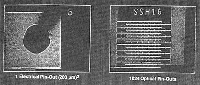
Figure 1.
One thousand twenty-four optical connections contained within the same
area as one electronic connection.
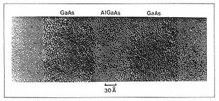
Figure 2.
Plus or minus one atomic layer precision of molecular beam epitaxy.
we can grow optical components such as mirrors. If we change the recipe, we can grow quantum wells, which give the material unusual optical properties. We can also grow p-n junctions to make electronic. This process of MBE gives us a way of integrating optics, materials, and electronics at an atomic level, which blurs the traditional distinction between electronics and optics.
One of the devices developed on the basis of this technology is the SEED device (Prise et al. 1991), a light-controlled mirror that we can toggle between 10 and 60 per cent reflectivity. These devices function as flip-flop with optical inputs and outputs. We have fabricated arrays of up to 32K devices and have run some of these devices at one gigahertz
A second device based on MBE is the microlaser (Jewell et al. 1991). MBE was used to grow a mirror, a quantum well, and then a second mirror. We can then fabricate millions of lasers by etching the wafer. This is shown in Figure 3. Our yield is over 95 per cent, and the raw cost is approximately $0.0001 per laser. The yields and cost of this process will dramatically affect the availability of lasers. This technology is useful in terms of the connectivity of optics because it demonstrates that thousands of lasers can be fabricated in a very small area.
A second reason for using optics is the bandwidth. An optical channel has over one terahertz of bandwidth. A thousand channels, each at one gigabit per second, can also be accomplished by using wavelength division multiplexing techniques to break this bandwidth into thousands of individual channels. The microlasers shown in Figure 3 can also be used in this manner. These wafers can be grown on a slight slant. This technique would make each of the microlasers function at a slightly different wavelength.
One of the problems with trying to achieve a thousand interconnects, each at one gigabit per second, is the optical packaging. In electronics the circuit boards, sockets, etc., are quite standardized. Optical setups have usually been one of a kind and quite large, with many micrometer adjustments. We have directed a large part of our effort at miniaturizing and simplifying this packaging. Our first system took three optical benches, each 4 by 12 feet, to interconnect three optical logic gates. The next year, we were able to reduce this to a 1- by 1-foot module that interconnected 32 gates. A year later, we interconnected four of these 1- by 1-foot modules to build a simple optical pipelined processor (Prise et al. 1991). See Figure 4. Six months later, another group hooked three 8-by-8 arrays of optical logic gates together with a 2- by 3-foot setup. A year later, they interconnected six arrays, each 32 by 32, with a 1- by 1-foot system. We have since managed to reduce most of the optics in our
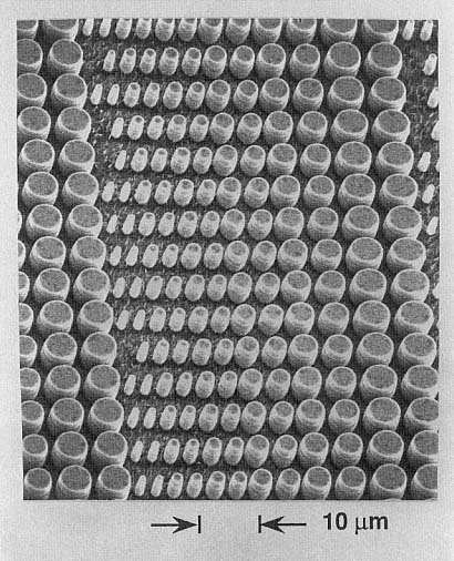
Figure 3.
An array of surface emitting microlasers.
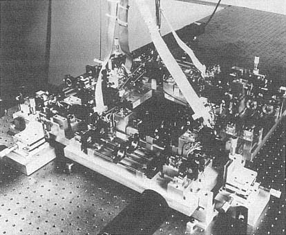
Figure 4.
A simple optical pipelined processor.
original 1- by 1-foot module to a module 1 by 2 by 3 inches in size (Figure 5).
We are now trying to reduce most of the optics in our original 1- by 1-foot module so that it fits onto the surface of a quarter. This technology, three-dimensional planar optics (Streibl et al. 1989), basically replaces the lenses with holograms of the lenses and fabricates these holograms with photolithography (Figure 6). We have demonstrated complex optical systems with lenses capable of conveying a 32 by 32 array of spots with greater than a 90 per cent diffraction efficiency.
One Connection at One Terabit per Second
Another reason for trying to use optics is for its speed. Optical nonlinearities have been measured down to the femtosecond (10-15 s), whereas electronics, because of the mobility of electrons in a semiconductor, has a built-in limit at around 10 picoseconds (10-12 s). The large bandwidths also allow us to go ultrafast. It frees us from the inductive and capacitive limitations of electronics. We have recently demonstrated an all-optical fiber logic AND gate, a NOT gate, a XOR gate, a 1.6-terahertz
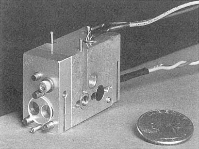
Figure 5.
A miniaturized version of one of the modules of the simple optical processor.
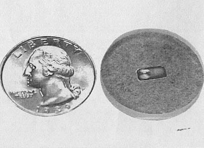
Figure 6.
An example of three-dimensional planar optics.
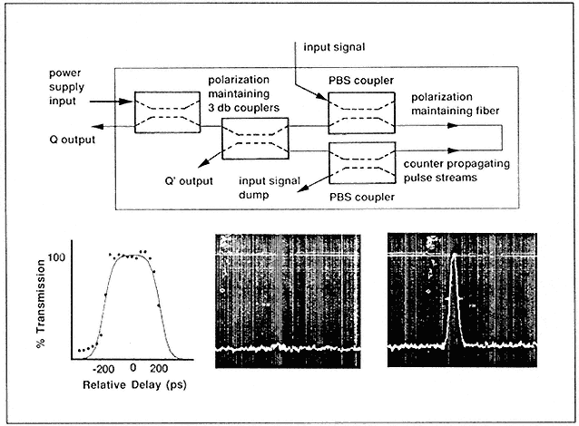
Figure 7.
An ultrafast all-optical fiber logic gate.
optical clock, a 2.5-gigabits-per-second multiplexer (Whitaker et al. 1991), and a 254-bit optical dynamic RAM (Figure 7). This is the beginning of a new digital technology that has the potential of working in the terahertz regime.
References
J. L. Jewell, J. P. Harbison, A. Scherer, Y. H. Lee, and L. T. Florez, "Vertical-Cavity Surface-Emitting Lasers: Design, Growth, Fabrication, Characterization," IEEE Quantum Electronics27 , 1332-1346 (1991).
M. E. Prise, N. C. Craft, M. M. Downs, R. E. LaMarche, L. A. D'Asaro, L. M. Chirovsky, and M. J. Murdocca, "Optical Digital Processor Using Arrays of Symmetric Self-Electro-optic Effect Devices," Applied Optics30 , 2287-2296 (1991).
N. Streibl, K. Brenner, A. Huang, J. Jahns, J. Jewell, A. W. Lohmann, D. A. B. Miller, M. Murdocca, M. E. Prise, and T. Sizer, "Digital Optics," Proceedings of the IEEE77 (12), 1954-1969 (1989).
N. A. Whitaker, Jr., H. Avramopoulos, P. M. W. French, M. C. Gabriel, R. E. LaMarche, D. J. DiGiovanni, and H. M. Presby, "All-Optical Arbitrary Demultiplexing at 2.5 Gbits/s with Tolerance to Timing Jitter," Optics Letters16 , 1838-1840 (1991).