Digital Superconductive Electronics
Fernand Bedard
Fernand D. Bedard graduated magna cum laude from Fordham University with a B.S. degree in physics and mathematics and received his Ph.D. in physics from Johns Hopkins University, where he held an NSF fellowship. He subsequently taught physics at the University of Cincinnati and, since coming to the Washington, DC, area, has taught at American University and the University of Maryland. He has authored or coauthored 25 publications in areas of microwave spectroscopy, optical pumping, superconductivity, and semiconductors.
He is currently a Fellow at the National Security Agency (NSA) Research and Engineering organization and is a Special Assistant to the Chief of Research at that organization. Immediately before taking up these posts, he served as Program Manager for Technology Base Research and Development, which provides for anticipating NSA's future mission requirements. Prior assignments included the directorship of both the NSA Office of Research Physics Division and of the Office of Research, itself.
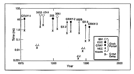
One of the major ingredients in the continual improvement of high-performance computers has been the increase in clock rate of the machines (Figure 1). The upper symbols show the clock interval of representative computers as they have evolved. Below each of these points is shown the gate delay of the logic devices, 10 to 20 times smaller
Figure 1.
Trends in logic speed.
than the clock interval, to allow multiple logic levels, package delay, and skew to be accommodated. At the lower left is a data point, circa 1978, of an exploratory superconductive device whose fully loaded gate delay was roughly 50 picoseconds at that time; obviously today there is no computer that reflects that device's performance. A major effort to bring that about in the U.S. was terminated several years later.
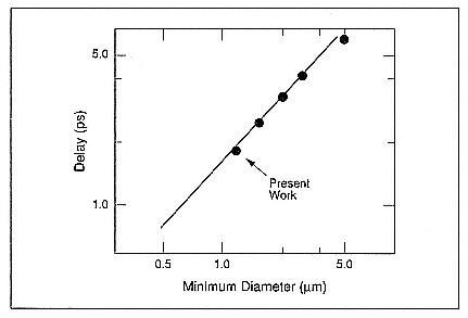
At just about that time, the Ministry of International Trade and Industry (MITI) in Japan established a Superspeed Project—of which superconductive devices were an element—whose goal was to demonstrate an advanced computer that used nonsilicon technology. Out of this work came some very impressive results from the major participants, Hitachi, Fujitsu, Nippon Electric Corporation (NEC), and MITI's Electro Technical Laboratory. Fujitsu's work is particularly noteworthy. They demonstrated astounding chip-level performance by first building the functionality of an AMD 2901 on a chip that operated with the characteristics shown in Table 1. They proudly pointed out that the chip power dissipation, five milliwatts, was equal to the power of a single gate of the fastest semiconductor competitor. The 2.5-micrometer feature size was reduced to 1.5 micrometers to demonstrate gate performance (Figure 2)—near one-picosecond delay. Using 1.5-micrometer lithography, they then shrank the microprocessor onto approximately one-third of the five-millimeter-square chip, added more memory, and repeated the demonstration, achieving the results shown in Table 2. Notice that the gate complexity is roughly 3000 gates with a six-milliwatt power consumption—about two microwatts per gate. The next chip demonstration
| ||||||||||||||||||||||||
Figure 2.
Gate delay versus junction diameter (Fujitsu, August 1988).
| ||||||||||||||
was of a digital signal-processor chip, again using 1.5-micrometer feature size. This time the gate count was 6300, the clock rate was one gigahertz, and once more the power consumption was low—12 milliwatts, or again about two microwatts per gate (Tables 3 and 4).
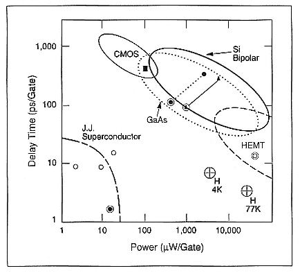
If you look at the usual delay-versus-power plot (Figure 3) to size up the comparisons, you find that silicon, as represented by NEC's SX-3, and gallium arsenide, as planned by the CRAY-3, are in the 70–80-picosecond unloaded-gate-delay regime and 250-picosecond loaded-gate-delay regime. The gate power consumption is in the milliwatts-per-gate domain, whereas the Fujitsu demonstrations are in the microwatts-per-gate domain for power while providing sub-10-picosecond loaded gate delay.
| ||||||||||||||||||||||
| ||||||||||||||
Figure 3.
Comparisons of delay versus power for digital superconducting, semiconducting
gate, and circuit.
What about factoring in the refrigerator power, approximately 500 to 1000 times the required computer logic power consumption? First, even accounting for that produces a faster chip performance-per-watt total and, more importantly, puts the power consumption where it is easily dealt with—at the unregulated power line, not at the tightly packed (for high-speed clocks) logic engine. Furthermore, the cooling and power supply requirements of conventional technology are rarely referred to and factored in at the system level.
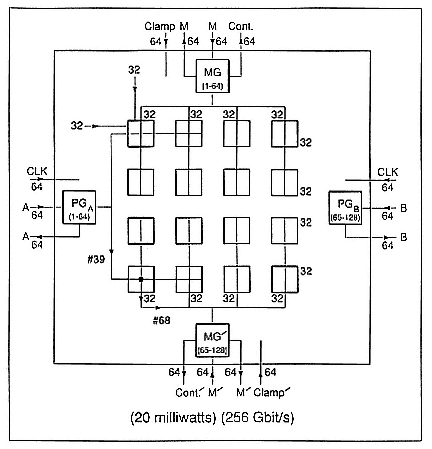
There is an effort under way presently to demonstrate a switching network, a crossbar, using superconductive devices in such a way as to exploit their high speed and very low power, along with the advantage of zero-resistance transmission lines. The prototype, a 128-×-128 crossbar (Figure 4), is designed to switch two gigabits per second of data per serial channel, with room temperature inputs and outputs. The power dissipation at 4K should be 20–40 milliwatts and, even with a refrigerator
Figure 4.
Pathway through a 128-×-128 crossbar (32-×-32 chip).
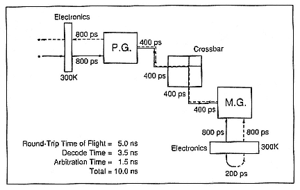
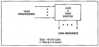
"penalty," would be a small fraction of the room-temperature electronics it services and would be much lower than any semiconductor competitor of lesser performance. The round trip "request-acknowledge" time should be approximately 10 nanoseconds, including address and arbitration time (Figure 5). If successful, the architecture, which depends intrinsically upon the devices, should allow the building of a 1024-×-1024 crossbar (Figure 6) with substantially the same access times as the 128-×-128 crossbar. The system's speed limitation is determined by the speed of light and the inability of semiconductors to keep up.
Figure 5.
Timing through crossbar, from processor to memory and back.
Figure 6.
A 1024-×-1024 crossbar switch.
