2—
TECHNOLOGY PERSPECTIVE
This session focused on technology for supercomputing—its current state, projections, limitations, and foreign dependencies. The viability of the U.S. semiconductor industry as a source of parts was considered. The possible roles of gallium arsenide, silicon, superconductive, and electro-optical technologies in supercomputers were discussed. Packaging, cooling, computer-aided design, and circuit simulation were also discussed.
Session Chair
Robert Cooper,
Atlantic Aerospace Electronics Corporation
Overview
Robert Cooper
Robert Cooper is currently the President, CEO, and Chairman of the Board of Atlantic Aerospace Electronics Corporation. Previously, he served simultaneously as Assistant Secretary of Defense for Research and Technology and Director of the Defense Advanced Research Projects Agency (DARPA). Under his directorship, DARPA moved into areas such as programs in advanced aeronautical systems, gallium arsenide microelectronic circuits, new-generation computing technology, and artificial intelligence concepts. Bob has also been the Director of the NASA Goddard Space Flight Center and the Assistant Director of Defense Research at MIT's Lincoln Laboratory. Bob holds a doctorate from MIT in electrical engineering and mathematics.
When I was at Goddard, we started the first massively parallel processor that was built, and it subsequently functioned at Goddard for many, many years. Interestingly enough, as I walked into this room to be on this panel, one of the folks who was on that program sat down next to me and said that he remembered those days fondly.
I'm really quite impressed by this group, and I subscribe to the comment that I heard out in the hallway just before the first session. One person was talking to another and said that he had never seen such a high concentration of computing genius in one place since 1954 at the Courant Institute, when John von Neumann dined alone. Be that as it may, I am nevertheless confident that if anything can be made to happen in the
high-end computer industry in this country, this group can play a key role in making it happen.
That comment also goes for the panel today, which is going to attack the problems of technology and perspectives for the future. We actually are starting this conference from a technical perspective by looking at the future—considering the prospects for computation—rather than looking toward the past, as we did in the first session.
Before we get started with our first speaker, I'd like to say a couple of words about what I see happening to the technology of high-end computing in the U.S. and in the world. Basically, the enabling technologies for high-end computing are the devices themselves. The physical constraints are the things that you will hear a lot about in this session: the logic devices; the memory devices; the architectural concepts, to a certain extent, which are determined by how you can fit these things together; and the interconnect technologies.
The main issue with technology developments in this area in this country is that we are somehow unable to take advantage of all of these things at the scale required to put large-scale systems together, and that is one of the reasons why we started the Strategic Computing Initiative back in 1983 at the Defense Advanced Research Projects Agency (DARPA), and that is why I think we are all hanging so much hope on the High Performance Computing Initiative that has come out of the study activity at DARPA and at the Office of Science and Technology Policy since about 1989.
I think it is the technology transition problem that we have to face. There is a role for government and a role for industry in the transition. I have been associated with some companies recently who have tried to take technology that they developed or that was somewhat common in the industry and make products out of it. I think that before we finish this particular session, we should talk about the issue of technology transition.
Supercomputing Tools and Technology
Tony Vacca
Tony Vacca is the Vice President of Technology at Cray Research, Inc., and has responsibility for product and technology development beyond Cray's C90 vector processor. Tony has had over 20 years' experience with circuit design, packaging, and storage. He began his career working at Raytheon Company as a design engineer, thereafter joining Control Data Corporation. From 1981 to 1989, he was the leader of the technology group at Engineering Technology Associates Systems. Tony has a bachelor of science degree in electrical engineering from the Michigan Technological Institute and has done graduate work at Northeastern and Stanford Universities.
The supercomputer technologies, or more generally, high-performance computer technologies, cover a broad spectrum of requirements that have to be looked at simultaneously at any given time to meet the goals, which are usually schedule-driven.
From a semiconductor perspective, the technologies fall into four classes: silicon, gallium arsenide, the superconductor, and the optical. In parallel, we have to look simultaneously at such things as computer-aided design tools, under which is a category of elements that get increasingly important as microminiaturization and scaling of integration rise.
Also, we have to look at the packaging issues, and there are a lot of computer-aided design tools that are helping us in that area. As was
discussed earlier, the issue of thermal management at all levels is very crucial, but the need for performance still dominates; we have to keep that in perspective.
Silicon is a very resilient technology, and every time it gets challenged it appears to respond. There are a lot of challenges to silicon, but I don't see many candidates in the near future that are more promising in the area of storage, especially dynamic storage, and possibly in some forms of logic.
Gallium arsenide has struggled over the last 10 years and is finally coming out as a "real" technology. Gallium arsenide has sent some false messages in some forms because some of the technology has focused not on performance but on power consumption. When it focuses on both, it will be much more effective for us. Usually when we are applying these technologies, we have to focus on the power and the speed simultaneously, especially because we are putting more processors on the floor.
The optical technology, from our viewpoint, has been used a lot in the communications between various mediums. When people talk about multigigahertz operations, I have some difficulty because I'm fighting to get 500-megahertz, single-bit optics in production from U.S. manufacturers. When people talk about the ability of 20-, 50-, 100-, and 500-gigabit-per-second channels, I believe that is possible in some form, but I don't know how producible the concept is.
Cryogenic technology was fairly successful several years ago. Cryogenic technology is a superconductive Josephson junction technology that also needs significant help to bring it to viable production; to apply it, one needs a catalyst that the other two technologies are beginning to have.
Interestingly, there may be some people that believe that if you escape an architecture that is massively parallel, you can escape advancing technology. I think switching does not change the focus at all to a need for high-performance technology because the massively parallel entry points are the points of entrance and not the points of completion. If we lose focus across a 10-year span, we will have fooled ourselves into believing that we have defocused semiconductor technology, logic, packaging, or interconnect technology. I think we will have to have high-performance technology to stay in the leadership position that we are in.
In the interests of our position of leadership, I have been keeping what I call a U.S.-Japan technology "score card" (Figure 1). Design tools, packaging, integrated-circuit chips, and semiconductor capital equipment are the primary technology categories. The boxes under those categories in Figure 1 indicate where I think we are, relative to Japan, in
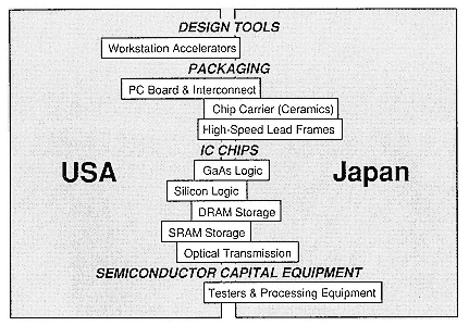
Figure 1.
USA-Japan technology "score card."
these particular technological areas. These are key areas that I think we sometimes avoid developing. However, we must concentrate on these areas and areas of technology like these because they are the basis for developing the technologies we can build products from.
We cannot select technologies "à la carte" and discount other technologies. Technologies must be selected and balanced against one another. In the past, we didn't focus so much on supercomputer technologies because supercomputers a few years ago were alive and well, and a few companies were carrying the ball. A few years ago we didn't focus on semiconductor technologies because they were alive and well, and we were doing such a good job.
Now there is the capital issue that I think is very significant. If you consider the extent to which major semiconductor suppliers in the U.S. today depend on foreign capital equipment for getting their jobs done, then you appreciate that we are facing a very crucial issue.
High-Performance Optical Memory Technology at MCC
John Pinkston
John Pinkston was the Vice President and Director of the Exploratory Initiatives Program at the Microelectronics and Computer Technology Corporation. Currently, he is a Research and Development Fellow at the National Security Agency. Dr. Pinkston received a bachelor's degree in electrical engineering from Princeton University and a Ph.D., also in electrical engineering, from MIT.
During this session we are going to hear about high-speed devices for logic, memory, and packaging, which are necessary and critical to build any high-performance supercomputing system. I would like to talk about a high-performance bulk-storage technology that we have been working on at the Microelectronics and Computer Technology Corporation (MCC), which, if it is successful, could impact very significantly the performance of supercomputer systems that deal with data-intensive projects.
Specifically, I am talking about volume holographic storage. Picture in your mind a disk that has a latency time of 10 microseconds and an I/O transfer of about a gigabit per second. That is the kind of technology that would impact environments where "solid-state disks" are used today.
Basically what we are working on is optical technology—storing a hologram for an array of bits in a photosensitive crystal in the form of a two-dimensional page. The motivation for MCC's involvement with
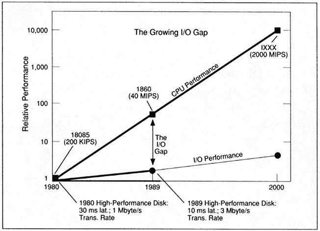
Figure 1.
Why MCC got involved with holographic storage.
holographic storage is the widening gap between CPU and I/O performance (Figure 1). In areas where the problem is data intensive and data limited, the I/O performance is the limiting factor of the performance of the overall system.
The concept is shown in Figure 2. Data are brought in and stored in a spatial light modulator, which is essentially a square array of spots that are transparent or opaque. The modulator is illuminated by a light from a laser and is then imaged onto a photosensitive crystal, with about a one-millimeter-square area. The pattern is interfered with by a reference beam from the same laser brought in at an angle, which creates an interference pattern or a hologram in this area of the crystal material.
The crystal is a photorefractive material that stores an image. The interference pattern, which has areas of high intensity and low intensity, creates a local change in the index of refraction where the light intensity is high (Figure 3). Essentially, electrons get excited into mobile states and settle back down where the light intensity is not so great. If the light is taken away, the electrons freeze in some trapping states, and you are left with essentially a charge grating written in the material that persists and contains the hologram of the image.
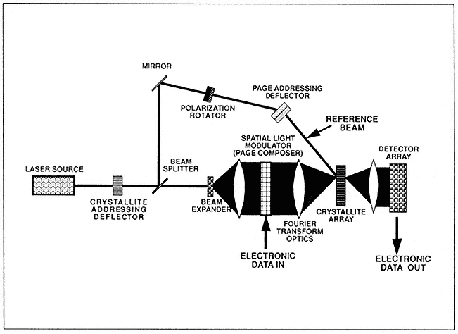
Figure 2.
Optical configuration of the hologram concept.
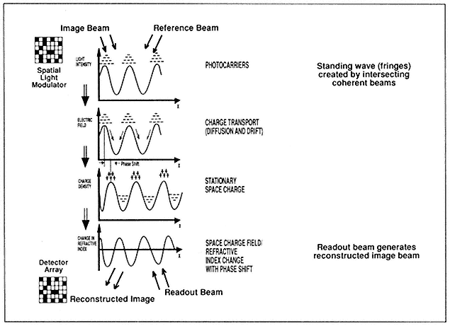
Figure 3.
Photorefractive recording.
To read data, the crystallite array is illuminated with the reference beam, which scatters off the diffraction grating, reconstructs the object beam, and is imaged onto a detector array such as a charge-coupled device (CCD). One can store many pages into the same volume of material, as with holograms, by varying the angle of the incoming beam and therefore varying the spacing of the grating. You can think of it as spatial frequency division multiplexing of signals superimposed in the same module.
We have seen storage in the range of 30 to 50 pages in a region that we call a stack, and you can have multiple stacks in nonoverlapping volumes of the crystal.
Readout can occur in the 10-microsecond time frame. Writing takes a little longer—in the 100-microsecond time frame.
This technology offers potential storage density in the gigabyte range. This density is not really going to compete with very large archival disks but is very competitive with high-performance disks today. This idea has been around for a while, for probably 20 years, but recent developments have made it more attractive than before.
The problems in the past had been that, first, the material was very difficult to work with. We use a strontium barium niobate. One can also use a bismuth silicon oxide. These are both very hard materials to obtain in sufficient purity and quality.
Second, there was a problem that no one had been able to overcome. Both reads and writes illuminate the crystal and cause some fading of the holograms in that stack.
Basically, in our lab we have developed a way of making the crystal by stacking up a bunch of fibers, which can be grown much more easily than a large bulk crystal, thereby getting around the material-availability problem. Further, we've produced a nondestructive readout technique. Figure 4 lists the innovations MCC has patented in the fields of crystallite-array and nondestructive-readout technology.
The technology is now quite promising. Performance projections are targeted in the $1 to $20 per megabyte range, with multiple hundreds of megabits per second I/O rates and read latency in the microsecond time frame (Figure 5). Capacity is somewhere in the gigabyte range.
We feel we have to be able to beat what semiconductors can do at the system level by probably about five to 10 times in terms of cost per bit in the year in which our product becomes available.
We have built up a small functioning unit that has potential. It is about a foot on a side and has a laser, two acousto-optic deflectors, several mirrors and lenses, a spatial light modulator, a storage crystal, and a CCD
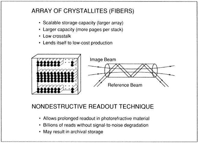
Figure 4.
MCC-patented innovations in two key Holostore technologies.
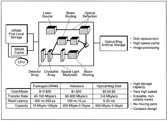
Figure 5.
Performance projections.
| ||||||||||||||||||||||||||||||||||||||||
Figure 6.
Bobcat II project
detector array. The unit is hooked up to a PC and is operating. We plan to develop a prototype (Bobcat II) that we hope to have available by the end of 1992. The capabilities of Bobcat II are outlined in Figure 6.
Applications for the unit will include the following:
• disk drive replacement,
• high-speed cache memory,
• high-speed storage with direct optical interfaces to fiber-optic communications networks,
• high-speed image-acquisition processing,
• survivable mass storage for demanding environments, and
• optical computing.
Digital Superconductive Electronics
Fernand Bedard
Fernand D. Bedard graduated magna cum laude from Fordham University with a B.S. degree in physics and mathematics and received his Ph.D. in physics from Johns Hopkins University, where he held an NSF fellowship. He subsequently taught physics at the University of Cincinnati and, since coming to the Washington, DC, area, has taught at American University and the University of Maryland. He has authored or coauthored 25 publications in areas of microwave spectroscopy, optical pumping, superconductivity, and semiconductors.
He is currently a Fellow at the National Security Agency (NSA) Research and Engineering organization and is a Special Assistant to the Chief of Research at that organization. Immediately before taking up these posts, he served as Program Manager for Technology Base Research and Development, which provides for anticipating NSA's future mission requirements. Prior assignments included the directorship of both the NSA Office of Research Physics Division and of the Office of Research, itself.
One of the major ingredients in the continual improvement of high-performance computers has been the increase in clock rate of the machines (Figure 1). The upper symbols show the clock interval of representative computers as they have evolved. Below each of these points is shown the gate delay of the logic devices, 10 to 20 times smaller
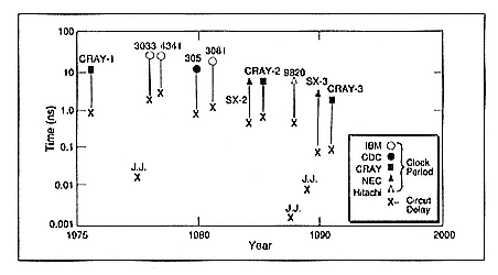
Figure 1.
Trends in logic speed.
than the clock interval, to allow multiple logic levels, package delay, and skew to be accommodated. At the lower left is a data point, circa 1978, of an exploratory superconductive device whose fully loaded gate delay was roughly 50 picoseconds at that time; obviously today there is no computer that reflects that device's performance. A major effort to bring that about in the U.S. was terminated several years later.
At just about that time, the Ministry of International Trade and Industry (MITI) in Japan established a Superspeed Project—of which superconductive devices were an element—whose goal was to demonstrate an advanced computer that used nonsilicon technology. Out of this work came some very impressive results from the major participants, Hitachi, Fujitsu, Nippon Electric Corporation (NEC), and MITI's Electro Technical Laboratory. Fujitsu's work is particularly noteworthy. They demonstrated astounding chip-level performance by first building the functionality of an AMD 2901 on a chip that operated with the characteristics shown in Table 1. They proudly pointed out that the chip power dissipation, five milliwatts, was equal to the power of a single gate of the fastest semiconductor competitor. The 2.5-micrometer feature size was reduced to 1.5 micrometers to demonstrate gate performance (Figure 2)—near one-picosecond delay. Using 1.5-micrometer lithography, they then shrank the microprocessor onto approximately one-third of the five-millimeter-square chip, added more memory, and repeated the demonstration, achieving the results shown in Table 2. Notice that the gate complexity is roughly 3000 gates with a six-milliwatt power consumption—about two microwatts per gate. The next chip demonstration
| ||||||||||||||||||||||||
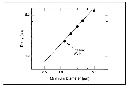
Figure 2.
Gate delay versus junction diameter (Fujitsu, August 1988).
| ||||||||||||||
was of a digital signal-processor chip, again using 1.5-micrometer feature size. This time the gate count was 6300, the clock rate was one gigahertz, and once more the power consumption was low—12 milliwatts, or again about two microwatts per gate (Tables 3 and 4).
If you look at the usual delay-versus-power plot (Figure 3) to size up the comparisons, you find that silicon, as represented by NEC's SX-3, and gallium arsenide, as planned by the CRAY-3, are in the 70–80-picosecond unloaded-gate-delay regime and 250-picosecond loaded-gate-delay regime. The gate power consumption is in the milliwatts-per-gate domain, whereas the Fujitsu demonstrations are in the microwatts-per-gate domain for power while providing sub-10-picosecond loaded gate delay.
| ||||||||||||||||||||||
| ||||||||||||||
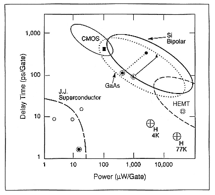
Figure 3.
Comparisons of delay versus power for digital superconducting, semiconducting
gate, and circuit.
What about factoring in the refrigerator power, approximately 500 to 1000 times the required computer logic power consumption? First, even accounting for that produces a faster chip performance-per-watt total and, more importantly, puts the power consumption where it is easily dealt with—at the unregulated power line, not at the tightly packed (for high-speed clocks) logic engine. Furthermore, the cooling and power supply requirements of conventional technology are rarely referred to and factored in at the system level.
There is an effort under way presently to demonstrate a switching network, a crossbar, using superconductive devices in such a way as to exploit their high speed and very low power, along with the advantage of zero-resistance transmission lines. The prototype, a 128-×-128 crossbar (Figure 4), is designed to switch two gigabits per second of data per serial channel, with room temperature inputs and outputs. The power dissipation at 4K should be 20–40 milliwatts and, even with a refrigerator
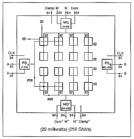
Figure 4.
Pathway through a 128-×-128 crossbar (32-×-32 chip).
"penalty," would be a small fraction of the room-temperature electronics it services and would be much lower than any semiconductor competitor of lesser performance. The round trip "request-acknowledge" time should be approximately 10 nanoseconds, including address and arbitration time (Figure 5). If successful, the architecture, which depends intrinsically upon the devices, should allow the building of a 1024-×-1024 crossbar (Figure 6) with substantially the same access times as the 128-×-128 crossbar. The system's speed limitation is determined by the speed of light and the inability of semiconductors to keep up.
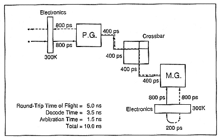
Figure 5.
Timing through crossbar, from processor to memory and back.
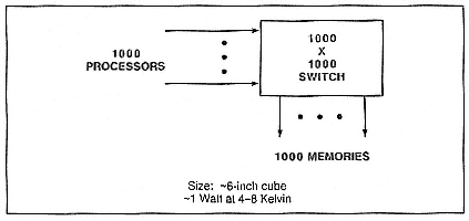
Figure 6.
A 1024-×-1024 crossbar switch.
Enabling Technology:
Photonics
Alan Huang
Alan Huang is head of the Digital Optics Research Department in the Communications Systems Research Laboratory at AT&T Bell Laboratories. He has been interested in optical computing for almost 20 years. Dr. Huang is also known for his contributions to very-large-scale integration and broadband communications networks. He received his Ph.D. in electrical engineering from Stanford University, Palo Alto, California. He has published over 50 papers and is the holder of 20 patents.
Introduction
Computers, as we know today, will be just be one component of an intellectual power grid in which computation and storage will become commodities traded over optical fiber "power lines." Success will hinge on the successful integration of computers, communications, and their associated technologies—electronics and photonics at both a macro and micro level.
At the micro level, the parallelism of optics is the most important factor. Architecturally, this connectivity can be used to transparently extend the name space and simplify the coordination of thousands of microprocessors into a unified micro-distributed computer. The goal is a thousand interconnections, each at one gigabit per second.
At the macro level, the bandwidth of optics is the most important parameter. Architecturally, this connectivity can be used to transparently extend the name space and simplify the coordination of thousands of computers into a unified macro-distributed computer. Our goal is one connection at a terabit per second.
A Thousand Interconnections, Each at One Gigabit per Second
One of the main reasons for trying to use optics is its connectivity. It is relatively easy for a lens to convey a 100-by-100 array of channels, each with the bandwidth of an optical fiber. This is shown in Figure 1. One thousand twenty-four optical connections can be implemented in the same space it takes to make one electronic connection.
One of the fundamental technologies that makes all of these optical interconnects possible is molecular beam epitaxy (MBE). This technology gives us the ability to grow crystals atom by atom with the precision of plus or minus one atomic layer over a two-inch wafer. See Figure 2. What good is this? By varying the thickness and elemental composition,
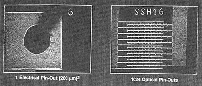
Figure 1.
One thousand twenty-four optical connections contained within the same
area as one electronic connection.
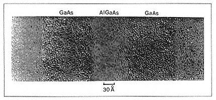
Figure 2.
Plus or minus one atomic layer precision of molecular beam epitaxy.
we can grow optical components such as mirrors. If we change the recipe, we can grow quantum wells, which give the material unusual optical properties. We can also grow p-n junctions to make electronic. This process of MBE gives us a way of integrating optics, materials, and electronics at an atomic level, which blurs the traditional distinction between electronics and optics.
One of the devices developed on the basis of this technology is the SEED device (Prise et al. 1991), a light-controlled mirror that we can toggle between 10 and 60 per cent reflectivity. These devices function as flip-flop with optical inputs and outputs. We have fabricated arrays of up to 32K devices and have run some of these devices at one gigahertz
A second device based on MBE is the microlaser (Jewell et al. 1991). MBE was used to grow a mirror, a quantum well, and then a second mirror. We can then fabricate millions of lasers by etching the wafer. This is shown in Figure 3. Our yield is over 95 per cent, and the raw cost is approximately $0.0001 per laser. The yields and cost of this process will dramatically affect the availability of lasers. This technology is useful in terms of the connectivity of optics because it demonstrates that thousands of lasers can be fabricated in a very small area.
A second reason for using optics is the bandwidth. An optical channel has over one terahertz of bandwidth. A thousand channels, each at one gigabit per second, can also be accomplished by using wavelength division multiplexing techniques to break this bandwidth into thousands of individual channels. The microlasers shown in Figure 3 can also be used in this manner. These wafers can be grown on a slight slant. This technique would make each of the microlasers function at a slightly different wavelength.
One of the problems with trying to achieve a thousand interconnects, each at one gigabit per second, is the optical packaging. In electronics the circuit boards, sockets, etc., are quite standardized. Optical setups have usually been one of a kind and quite large, with many micrometer adjustments. We have directed a large part of our effort at miniaturizing and simplifying this packaging. Our first system took three optical benches, each 4 by 12 feet, to interconnect three optical logic gates. The next year, we were able to reduce this to a 1- by 1-foot module that interconnected 32 gates. A year later, we interconnected four of these 1- by 1-foot modules to build a simple optical pipelined processor (Prise et al. 1991). See Figure 4. Six months later, another group hooked three 8-by-8 arrays of optical logic gates together with a 2- by 3-foot setup. A year later, they interconnected six arrays, each 32 by 32, with a 1- by 1-foot system. We have since managed to reduce most of the optics in our
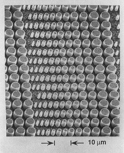
Figure 3.
An array of surface emitting microlasers.
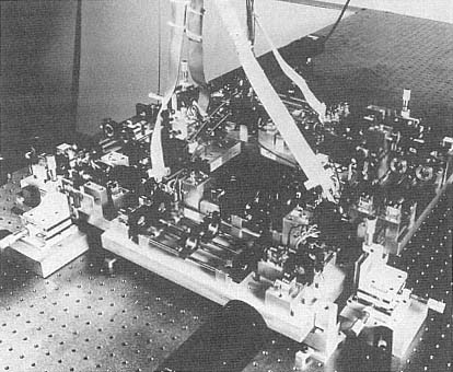
Figure 4.
A simple optical pipelined processor.
original 1- by 1-foot module to a module 1 by 2 by 3 inches in size (Figure 5).
We are now trying to reduce most of the optics in our original 1- by 1-foot module so that it fits onto the surface of a quarter. This technology, three-dimensional planar optics (Streibl et al. 1989), basically replaces the lenses with holograms of the lenses and fabricates these holograms with photolithography (Figure 6). We have demonstrated complex optical systems with lenses capable of conveying a 32 by 32 array of spots with greater than a 90 per cent diffraction efficiency.
One Connection at One Terabit per Second
Another reason for trying to use optics is for its speed. Optical nonlinearities have been measured down to the femtosecond (10-15 s), whereas electronics, because of the mobility of electrons in a semiconductor, has a built-in limit at around 10 picoseconds (10-12 s). The large bandwidths also allow us to go ultrafast. It frees us from the inductive and capacitive limitations of electronics. We have recently demonstrated an all-optical fiber logic AND gate, a NOT gate, a XOR gate, a 1.6-terahertz
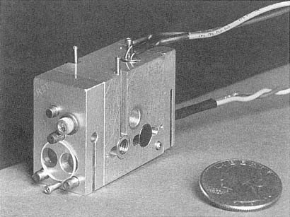
Figure 5.
A miniaturized version of one of the modules of the simple optical processor.
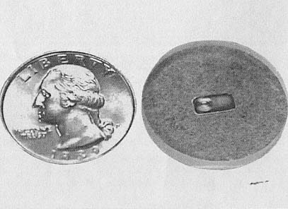
Figure 6.
An example of three-dimensional planar optics.
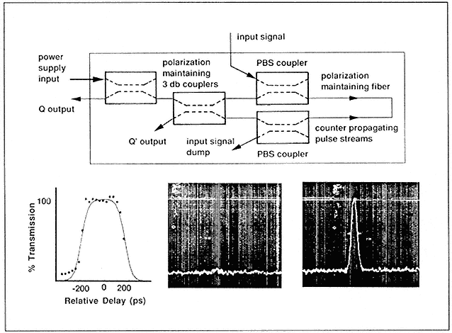
Figure 7.
An ultrafast all-optical fiber logic gate.
optical clock, a 2.5-gigabits-per-second multiplexer (Whitaker et al. 1991), and a 254-bit optical dynamic RAM (Figure 7). This is the beginning of a new digital technology that has the potential of working in the terahertz regime.
References
J. L. Jewell, J. P. Harbison, A. Scherer, Y. H. Lee, and L. T. Florez, "Vertical-Cavity Surface-Emitting Lasers: Design, Growth, Fabrication, Characterization," IEEE Quantum Electronics27 , 1332-1346 (1991).
M. E. Prise, N. C. Craft, M. M. Downs, R. E. LaMarche, L. A. D'Asaro, L. M. Chirovsky, and M. J. Murdocca, "Optical Digital Processor Using Arrays of Symmetric Self-Electro-optic Effect Devices," Applied Optics30 , 2287-2296 (1991).
N. Streibl, K. Brenner, A. Huang, J. Jahns, J. Jewell, A. W. Lohmann, D. A. B. Miller, M. Murdocca, M. E. Prise, and T. Sizer, "Digital Optics," Proceedings of the IEEE77 (12), 1954-1969 (1989).
N. A. Whitaker, Jr., H. Avramopoulos, P. M. W. French, M. C. Gabriel, R. E. LaMarche, D. J. DiGiovanni, and H. M. Presby, "All-Optical Arbitrary Demultiplexing at 2.5 Gbits/s with Tolerance to Timing Jitter," Optics Letters16 , 1838-1840 (1991).